
Current events
Next talk tomorrow at 11:00 by Adrian Miemczyk!
News 10.04.2026
New publication: Weak localization as a probe of spin-orbit-induced spin-split bands in bilayer graphene proximity coupled to WSe2
Site Content:
19.04.2025
New publication: Role of antisymmetric orbitals and electron-electron interactions on the two-particle spin and valley blockade in graphene double quantum dots
Phys. Rev. B 111, 165416 (2025) We report on an experimental study of spin and valley blockade in two-electron bilayer graphene (BLG) double quantum dots (DQDs) and explore the limits set by asymmetric orbitals and electron-electron interactions. The results obtained from magnetotransport measurements on two-electron BLG DQDs, where the resonant tunneling transport involves both orbital symmetric and antisymmetric two-particle states, show a rich level spectrum. We observe a magnetic field tunable spin and valley blockade, which is limited by the orbital splitting, the strength of the electron-electron interaction and the difference in the valley g-factors between the symmetric and antisymmetric two-particle orbital states. Our conclusions are supported by simulations based on rate equations, which allow the identification of prominent interdot transitions associated with the transition from single- to two-particle states observed in the experiment.

17.04.2025
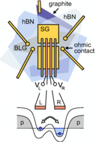
New publication: Gate-Defined Single-Electron Transistors in Twisted Bilayer Graphene
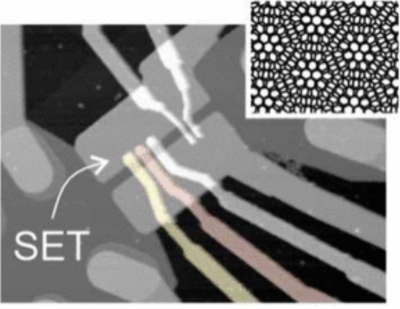
Nano Lett. 25, 6429 (2025) Twisted bilayer graphene (tBLG) near the magic angle is a unique platform where the combination of topology and strong correlations gives rise to exotic electronic phases. These phases are gate-tunable and related to the presence of flat electronic bands, isolated by single-particle band gaps. This enables gate-controlled charge confinements, essential for the operation of single-electron transistors (SETs), and allows one to explore the interplay of confinement, electron interactions, band renormalization, and the moiré superlattice, potentially revealing key paradigms of strong correlations. Here, we present gate-defined SETs in tBLG with well-tunable Coulomb blockade resonances. These SETs allow us to study magnetic field-induced quantum oscillations in the density of states of the source-drain reservoirs, providing insight into gate-tunable Fermi surfaces of tBLG. Comparison with tight-binding calculations highlights the importance of displacement-field-induced band renormalization crucial for future advanced gate-tunable quantum devices and circuits in tBLG including, e.g., quantum dots and Josephson junction arrays.
15.04.2025
New publication: Ultra-low-power cryogenic complementary metal oxide semiconductor technology

Nat. rev. electr. eng. 2, 277 (2025) Universal cryogenic computing, encompassing von Neumann, neuromorphic and quantum computing, paves the way for future big-data processing with high energy efficiency. Complementary metal oxide semiconductor (CMOS) technology operating at cryogenic temperatures with ultra-low power consumption is a key component of this advancement. However, classical CMOS technology, designed for room temperature applications, suffers from band-tail effects at cryogenic levels, leading to an increased subthreshold swing and decreased mobility values. In addition, threshold voltages are enlarged. Thus, classical CMOS technology fails to meet the low power requirements when cooled close to zero Kelvin. In this Perspective, we show that steep slope cryogenic devices can be realized by screening the band tails with the use of high-k dielectrics and wrap-gate architectures and/or reducing them through the optimization of the surfaces and interfaces within the transistors. Cryogenic device functionality also strongly benefits from appropriate source/drain engineering employing dopant segregation from silicides. Furthermore, the threshold voltage control can be realized with back-gating, work-function engineering and dipole formation. As a major implication, future research and development towards cryogenic CMOS technology requires a combination of these approaches to enable universal cryogenic computing at the necessary ultra-low power levels.
26.03.2025
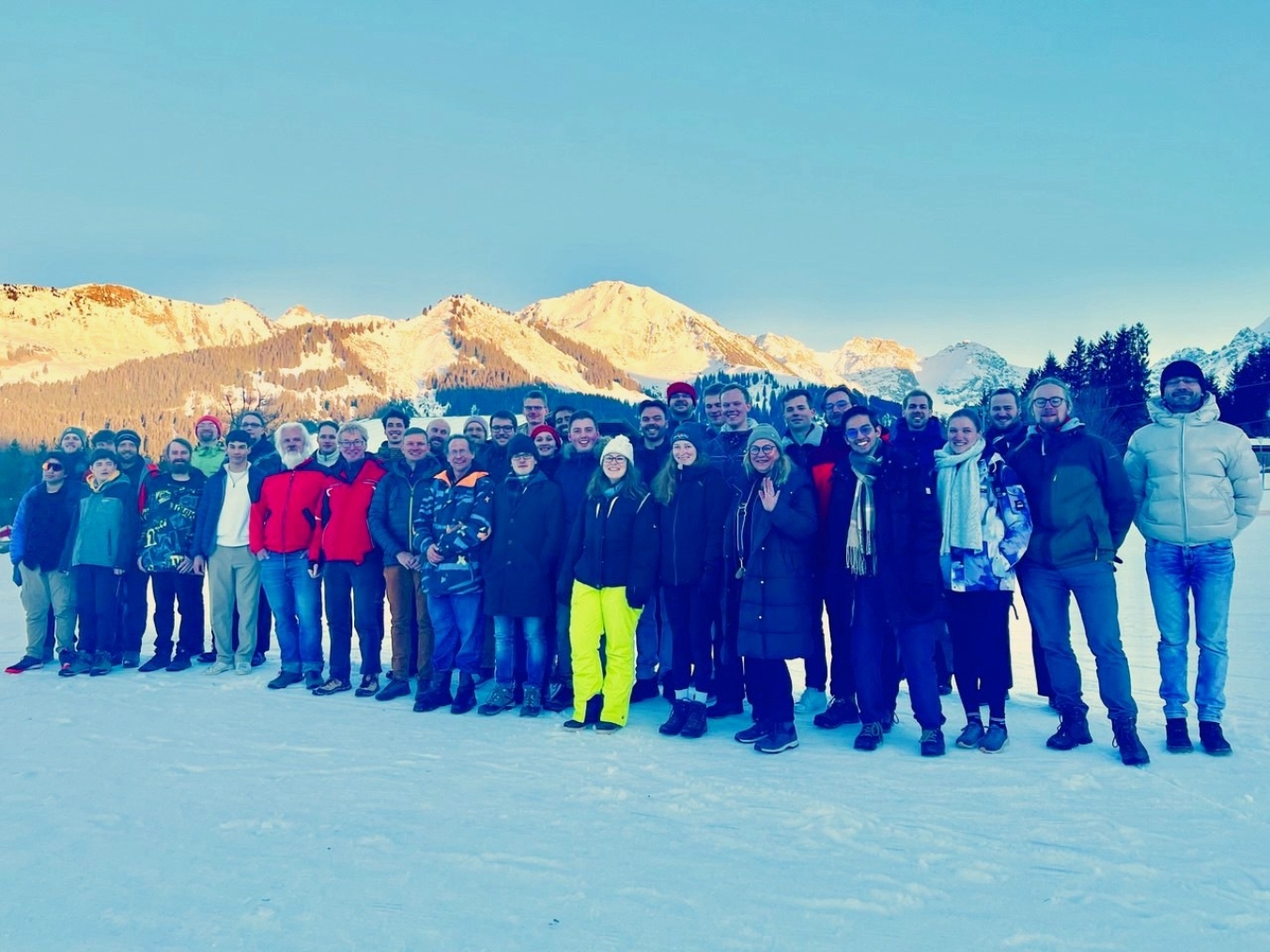
Söllerhaus-Workshop 2025
The Söllerhaus-Workshop 2025 from the 15th to the 22nd of March of the 2nd Institute of Physics A , B and C focusing on interesting (partly cross-sectional) topics was great fun with many interesting talks and discussions, good skiing and slippery snow hiking with torches.
25.03.2025
Poster prize for Alexander Rothstein at the "37th IWEPNM Kirchberg Winterschool"

Alexander Rothstein won one of the three poster prizes at the IWEPNM Winterschool in Kirchberg with his poster on "Gate-tunable Josephson diods in magic angle twisted bilayer graphene". Congratulations!
21.03.2025
New publication: Bluetooth sensors in phyphox with Arduino and MicroPython
A new publication by Staacks et al. about the Bluetooth interface of the physics education app "phyphox".
Abstract:
In order to extend the available sensors of smartphone experiments with cheap microcontroller-based external sensors, the smartphone experimentation app 'phyphox' has been extended with a generic Bluetooth Low Energy interface. Since its application requires an in-depth understanding of the underlying technologies, the direct use of that interface for educational purposes is limited. To avoid this difficulty, the functionality was encapsulated into an Arduino and MicroPython library. With these, also educators and learners with only rudimentary programming knowledge can integrate an app-based interface into microcontroller projects with only few lines of code. This opens a wide range of new learning opportunities, which are described exemplarily.
Published in Physics Education (preprint on arXiv)
25.02.2025
Timo Bißwanger successfully defended his PhD thesis
On Tuesday 25.02.2025, Timo Bißwanger successfully defended his PhD thesis. Congratulations to Dr. Timo Bißwanger on this fantastic accomplishment!
14.02.2025
New publication: Super-resolution imaging of nanoscale inhomogeneities in hBN-covered and encapsulated few-layer graphene
Adv. Sci. 18, 2409039 (2025) Encapsulating few-layer graphene (FLG) in hexagonal boron nitride (hBN) can cause nanoscale inhomogeneities in the FLG, including changes in stacking domains and topographic defects. Due to the diffraction limit, characterizing these inhomogeneities is challenging. Recently, the visualization of stacking domains in encapsulated four-layer graphene (4LG) has been demonstrated with phonon polariton (PhP)-assisted near-field imaging. However, the underlying coupling mechanism and ability to image subdiffractional-sized inhomogeneities remain unknown. Here, direct replicas and magnified images of subdiffractional-sized inhomogeneities in hBN-covered trilayer graphene (TLG) and encapsulated 4LG, enabled by the hyperlensing effect, are retrieved. This hyperlensing effect is mediated by hBN's hyperbolic PhP that couple to the FLG's plasmon polaritons. Using near-field microscopy, the coupling is identified by determining the polariton dispersion in hBN-covered TLG to be stacking-dependent. This work demonstrates super-resolution and magnified imaging of inhomogeneities, paving the way for the realization of homogeneous encapsulated FLG transport samples to study correlated physics.