Current events
Next talk tomorrow at 11:30 by Simone Sotgiu!
News 11.11.2025
New publication: Tailoring Phonon Polaritons in hBN with the Plasmonic Phase-Change Material In3SbTe2
Site Content:
09.07.2025
Visitors from Budapest at our group
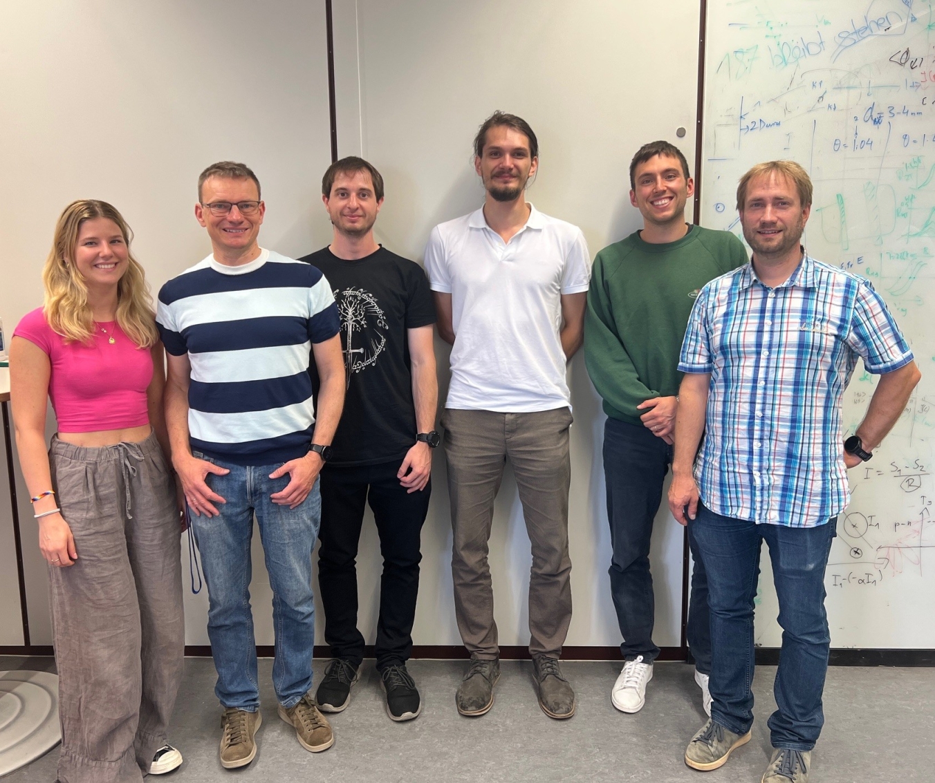
This week we had the pleasure of welcoming Rahimkulov Margarita and Bálint Szentpéteri from the Quantum Transport Laboratory of Szabolcs Csonka at Budapest University of Technology and Economics (BME). During their stay, they visited our labs and exchanged ideas with the bilayer graphene quantum dot team and others.

05.07.2025
New publication: Electric-Field-Tunable Spin−Orbit Gap in a Bilayer Graphene/WSe2 Quantum Dot
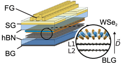
Nano Lett. 25 10549 (2025) We report on the investigation of proximity-induced spin–orbit coupling (SOC) in a heterostructure of bilayer graphene (BLG) and tungsten diselenide (WSe2). A BLG quantum dot (QD) in the few-particle regime acts as a sensitive probe for induced SOC. Finite bias and magnetotransport spectroscopy measurements reveal a significantly enhanced SOC that decreases with the applied displacement field, distinguishing it from pristine BLG. Furthermore, our measurements demonstrate a reduced valley g factor at larger displacement fields, consistent with weaker lateral confinement of the QD. Our findings show evidence of the influence of WSe2 across BLG layers, driven by reduced real-space confinement and increased layer localization of the QD states on the BLG layer distant to the WSe2 at higher displacement fields. This study demonstrates the electrostatic tunability of the spin–orbit gap in BLG/WSe2 heterostructures, which is especially relevant for the field of spintronics and future spin qubit control in BLG QDs.

06.06.2025
New publication:Anisotropic supercurrent suppression and revivals in a graphene-based Josephson junction under in-plane magnetic fields
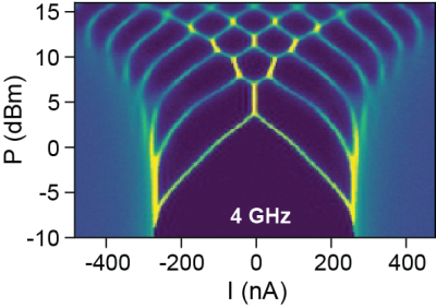
Phys. Rev. B 111, 245301 (2025) We report on a tunable Josephson junction formed by a bilayer graphene ribbon encapsulated in WSe2 with superconducting niobium contacts. We characterize the junction by measurements of the magnetic field–induced interference pattern and the AC Josephson effect manifested as Shapiro steps, examining current-dependent hysteresis and junction dynamics. The latter can be tuned by temperature, gate voltage, and magnetic field. Finally, we examine the evolution of the supercurrent when subjected to in-plane magnetic fields. Notably, we observe strong anisotropy in the supercurrent with respect to the orientation of the in-plane magnetic field. When the field is parallel to the current direction, the supercurrent is suppressed and shows revivals with increasing magnetic field, whereas it remains almost unaffected when the field is oriented in a perpendicular direction. We suggest that this anisotropy is caused by the dependence of supercurrent interference on the junction geometry.

22.05.2025
ML4Q Secures Continued Funding as Cluster of Excellence

The Cluster of Excellence Matter and Light for Quantum Computing (ML4Q) will continue to receive funding in the upcoming phase of Germany’s Excellence Strategy. This was announced today in Bonn by the German Council of Science and Humanities and the German Research Foundation (DFG). ML4Q is a joint research initiative between the University of Cologne (host university), the University of Bonn, RWTH Aachen University - with strong involvement of the 2nd Institute of Physics - and Forschungszentrum Jülich. The cluster addresses fundamental physical and technological challenges on the road to scalable and reliable quantum computing – from the development of high-performance qubits to modular architectures and the interface between quantum hardware and software. For more details see https://ml4q.de

05.05.2025
New publication: Terahertz photocurrent probe of quantum geometry and interactions in magic-angle twisted bilayer graphene
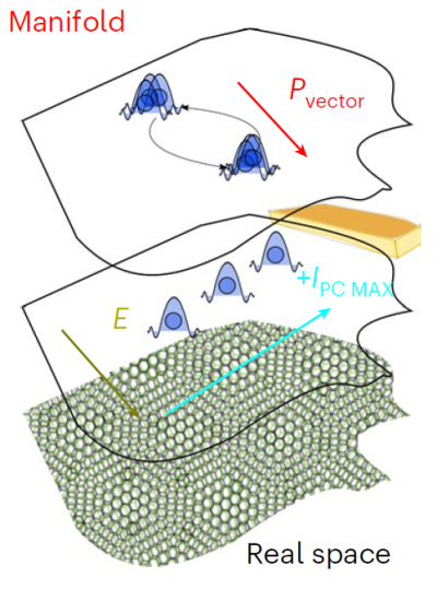
Nat. Mater. (2025) Moiré materials represent strongly interacting electron systems bridging topological and correlated physics. Despite notable advances, decoding wavefunction properties underlying the quantum geometry remains challenging. Here we utilize polarization-resolved photocurrent measurements to probe magic-angle twisted bilayer graphene, leveraging its sensitivity to the Berry connection that encompasses quantum ‘textures’ of electron wavefunctions. Using terahertz light resonant with optical transitions of its flat bands, we observe bulk photocurrents driven by broken symmetries and reveal the interplay between electron interactions and quantum geometry. We observe inversion-breaking gapped states undetectable through quantum transport, sharp changes in the polarization axes caused by interaction-induced band renormalization and recurring photocurrent patterns at integer filling factors of the moiré unit cell that track the evolution of quantum geometry through the cascade of phase transitions. The large and tunable terahertz response intrinsic to flat-band systems offers direct insights into the quantum geometry of interacting electrons and paves the way for innovative terahertz quantum technologies.

24.04.2025
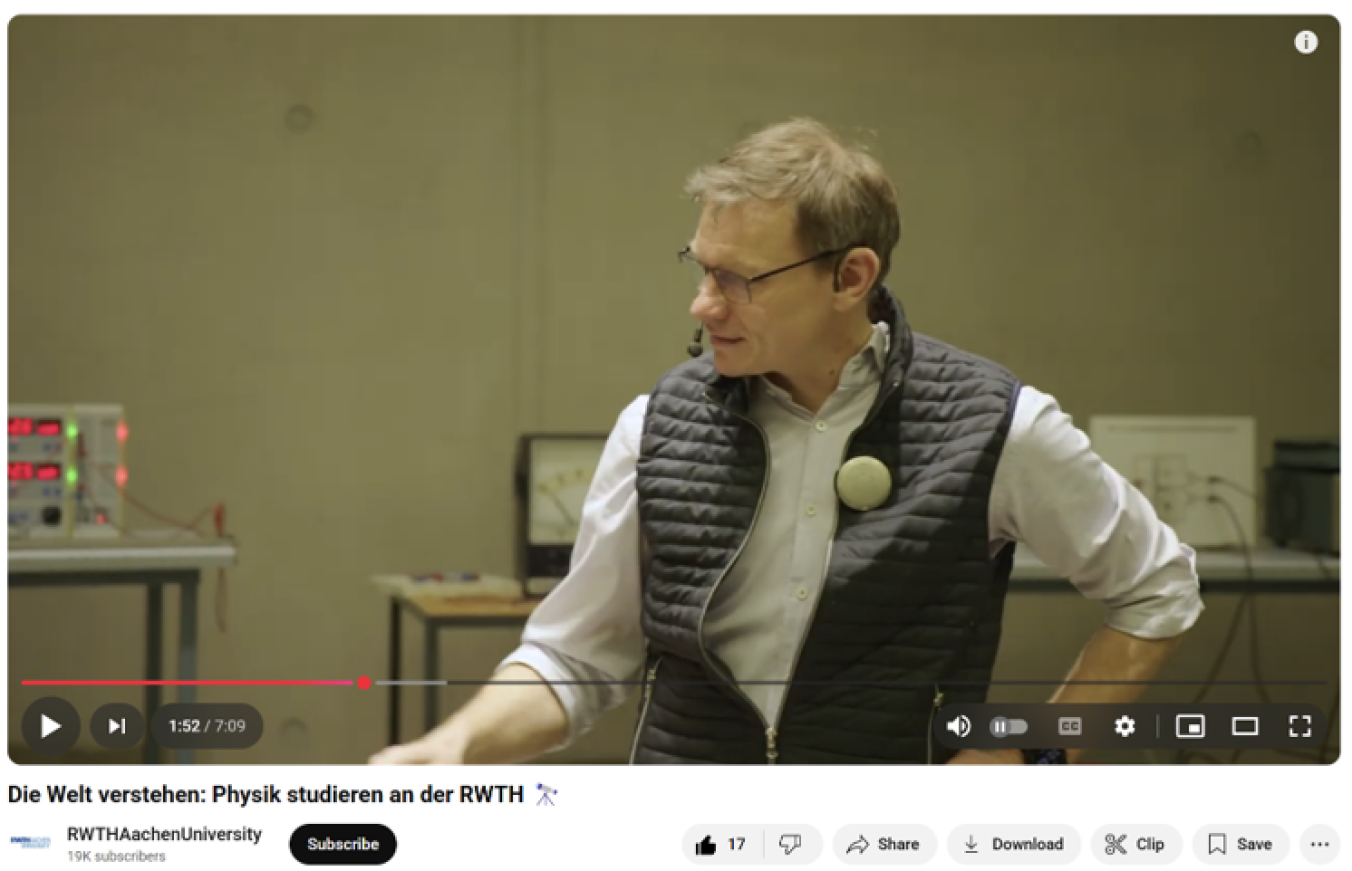
New short film about the physics programme at RWTH Aachen
There is a new short film about the physics programme at RWTH Aachen University (unfortunately only in German) which can be found here on youtube: https://www.youtube.com/watch?v=G7N0rrBHsWw Please forward to anyone who might be interested.

19.04.2025
New publication: Role of antisymmetric orbitals and electron-electron interactions on the two-particle spin and valley blockade in graphene double quantum dots
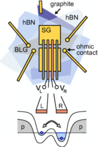
Phys. Rev. B 111, 165416 (2025) We report on an experimental study of spin and valley blockade in two-electron bilayer graphene (BLG) double quantum dots (DQDs) and explore the limits set by asymmetric orbitals and electron-electron interactions. The results obtained from magnetotransport measurements on two-electron BLG DQDs, where the resonant tunneling transport involves both orbital symmetric and antisymmetric two-particle states, show a rich level spectrum. We observe a magnetic field tunable spin and valley blockade, which is limited by the orbital splitting, the strength of the electron-electron interaction and the difference in the valley g-factors between the symmetric and antisymmetric two-particle orbital states. Our conclusions are supported by simulations based on rate equations, which allow the identification of prominent interdot transitions associated with the transition from single- to two-particle states observed in the experiment.

17.04.2025
New publication: Gate-Defined Single-Electron Transistors in Twisted Bilayer Graphene
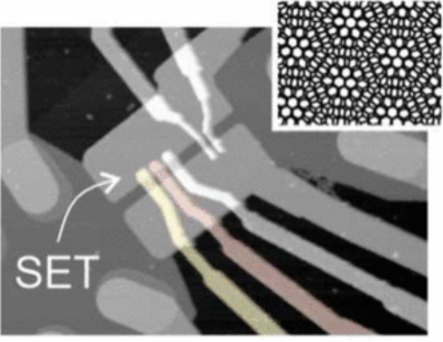
Nano Lett. 25, 6429 (2025) Twisted bilayer graphene (tBLG) near the magic angle is a unique platform where the combination of topology and strong correlations gives rise to exotic electronic phases. These phases are gate-tunable and related to the presence of flat electronic bands, isolated by single-particle band gaps. This enables gate-controlled charge confinements, essential for the operation of single-electron transistors (SETs), and allows one to explore the interplay of confinement, electron interactions, band renormalization, and the moiré superlattice, potentially revealing key paradigms of strong correlations. Here, we present gate-defined SETs in tBLG with well-tunable Coulomb blockade resonances. These SETs allow us to study magnetic field-induced quantum oscillations in the density of states of the source-drain reservoirs, providing insight into gate-tunable Fermi surfaces of tBLG. Comparison with tight-binding calculations highlights the importance of displacement-field-induced band renormalization crucial for future advanced gate-tunable quantum devices and circuits in tBLG including, e.g., quantum dots and Josephson junction arrays.

