
Current events
Next talk on Friday in 2 days by Yeganeh Mirzanejad.
News 05.07.2025
New publication: Electric-Field-Tunable Spin−Orbit Gap in a Bilayer Graphene/WSe2 Quantum Dot
Site Content:
19.01.2016
Poster prizes for Michael Schmitz and Jens Sonntag at the "Graphene Study 2016"
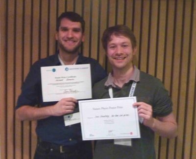
Michael Schmitz won the 1st poster prize and Jens Sonntag won the 3rd poster prize at the "Graphene Study 2016" in Les Houches (France). Congratulations!

15.01.2016
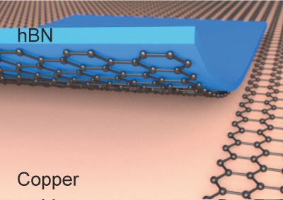
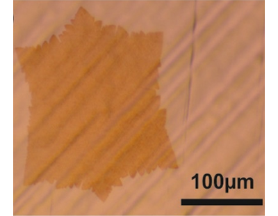
New publication: Ballistic transport exceeding 28 µm in CVD grown graphene
Nano Lett. 16, 1387 (2016)
We report on ballistic transport over more than 28 µm in graphene grown by chemical vapor deposition (CVD) that is fully encapsulated in hexagonal boron nitride. The structures are fabricated by an advanced dry van-der-Waals transfer method and exhibit carrier mobilities of up to three million cm2/(Vs). The ballistic nature of charge transport is probed by measuring the bend resistance in cross- and square-shaped devices. Temperature dependent measurements furthermore prove that ballistic transport is maintained exceeding 1 µm up to 200 K.
22.12.2015
RWTH Start-Up Grant for Johannes Güttinger
Johannes Güttinger receives a RWTH Start-Up Grant for his proposal for "hybrid quantum experiments with graphene membranes". Congratulation!
14.12.2015
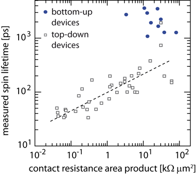
New publication: Spin and charge transport in graphene-based spin transport devices with Co/MgO spin injection and spin detection electrodes
Synthetic Metals, 210 Part A, 42 (2015)
Free online access until February 2, 2016 direct download
In this review we discuss spin and charge transport properties in graphene-based single-layer and few-layer spin-valve devices. We give an overview of challenges and recent advances in the field of device fabrication and discuss two of our fabrication methods in more detail which result in distinctly different device performances. In the first class of devices, Co/MgO electrodes are directly deposited onto graphene which results in rough MgO-to-Co interfaces and favor the formation of conducting pinholes throughout the MgO layer. We show that the contact resistance area product (RcA) is a benchmark for spin transport properties as it scales with the measured spin lifetime in these devices indicating that contact-induced spin dephasing is the bottleneck for spin transport even in devices with large RcA values. In a second class of devices, Co/MgO electrodes are first patterned onto a silicon substrate. Subsequently, a graphene-hBN heterostructure is directly transferred onto these prepatterned electrodes which provides improved interface properties. This is seen by a strong enhancement of both charge and spin transport properties yielding charge carrier mobilities exceeding 20,000 cm2/(Vs) and spin lifetimes up to 3.7 ns at room temperature. We discuss several shortcomings in the determination of both quantities which complicates the analysis of both extrinsic and intrinsic spin scattering mechanisms. Furthermore, we show that contacts can be the origin of a second charge neutrality point in gate dependent resistance measurements which is influenced by the quantum capacitance of the underlying graphene layer.
09.12.2015
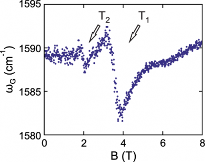
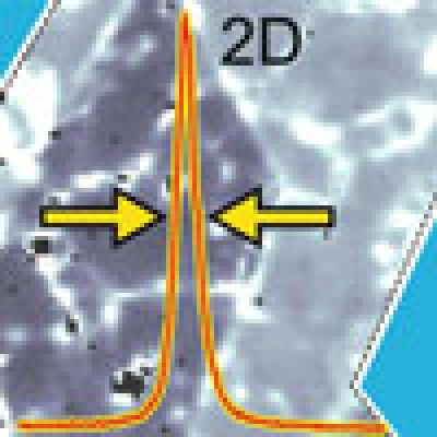
New publication: Probing electronic lifetimes and phonon anharmonicities in high-quality chemical vapor deposited graphene by magneto-Raman spectroscopy
Appl. Phys. Lett. 107, 233105 (2015)
We present a magneto-Raman study on high-quality single-layer graphene grown by chemical vapor deposition (CVD) that is fully encapsulated in hexagonal boron nitride by a dry transfer technique. By analyzing the Raman D, G, and 2D peaks, we find that the structural quality of the samples is comparable with state-of-the-art exfoliated graphene flakes. From B-field dependent Raman measurements, we extract the broadening and associated lifetime of the G peak due to anharmonic effects. Furthermore, we determine the decay width and lifetime of Landau level (LL) transitions from magneto-phonon resonances as a function of laser power. At low laser power, we find a minimal decay width of 140 cm−1 highlighting the high electronic quality of the CVD-grown graphene. At higher laser power, we observe an increase of the LL decay width leading to a saturation, with the corresponding lifetime saturating at a minimal value of 18 fs.
05.11.2015
New publication: Graphen auf dem Weg zur Anwendung
Physik in unserer Zeit 46, 269 (2015)
Graphen zeichnet sich durch eine Vielzahl von einzigartigen elektronischen,
optischen und mechanischen Eigenschaften aus und wird daher
zum Beispiel Magnetfeld-Hall-Sensoren oder Anwendungen in der
Hochfrequenztechnik und Optoelektronik deutlich verbessern. Unsere
Kollaboration des Forschungszentrums Jülich und der RWTH Aachen hat
ein neues Verfahren entwickelt, um synthetisch gewachsenes, hochqualitatives
Graphen herzustellen. Dies ist ein wichtiger Schritt, um graphenbasierte
Anwendungen zur Marktreife zu bringen.
29.09.2015
New publication: Raman Spectroscopy as Probe of Nanometer-Scale Strain Variations in Graphene
Nature Comm. 6, 8429 (2015)
Confocal Raman spectroscopy has emerged as a major, versatile workhorse for the non-invasive characterization of graphene. Although it is successfully used to determine the number of layers, the quality of edges, and the effects of strain, doping and disorder, the nature of the experimentally observed broadening of the most prominent Raman 2D line has remained unclear. Here we show that the observed 2D line width contains valuable information on strain variations in graphene on length scales far below the laser spot size, that is, on the nanometre-scale. This finding is highly relevant as it has been shown recently that such nanometre-scaled strain variations limit the carrier mobility in high-quality graphene devices. Consequently, the 2D line width is a good and easily accessible quantity for classifying the crystalline quality, nanometre-scale flatness as well as local electronic properties of graphene, all important for future scientific and industrial applications.
10.09.2015
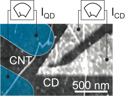
New publication: Back action of graphene charge detectors on graphene and carbon nanotube quantum dots
Physica Status Solidi B 252, 2461 (2015)
We report on devices based on graphene charge detectors (CDs) capacitively coupled to graphene and carbon nanotube quantum dots (QDs). We focus on back action effects of the CD on the probed QD. A strong influence of the bias voltage applied to the CD on the current through the QD is observed. Depending on the charge state of the QD, the current through the QD can either strongly increase or completely reverse as a response to the applied voltage on the CD. To describe the observed behavior, we employ two simple models based on single electron transport in QDs with asymmetrically broadened energy distributions of the source and the drain leads. The models successfully explain the back action effects. The extracted distribution broadening shows a linear dependency on the bias voltage applied to the CD. We discuss possible mechanisms mediating the energy transfer between the CD and QD and give an explanation for the origin of the observed asymmetry.