
Current events
Next talk on Friday in 3 days by Jonas Blum.
News 10.04.2026
New publication: Weak localization as a probe of spin-orbit-induced spin-split bands in bilayer graphene proximity coupled to WSe2
Site Content:
10.04.2026
New publication: Weak localization as a probe of spin-orbit-induced spin-split bands in bilayer graphene proximity coupled to WSe2
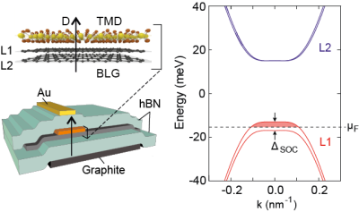
Phys. Rev. Applied 25, 044028 (2026) Proximity coupling of bilayer graphene (BLG) to transition metal dichalcogenides (TMDs) offers a promising route to engineer gate-tunable spin-orbit coupling (SOC) while preserving BLG’s exceptional electronic properties. This tunability arises from the layer-asymmetric electronic structure of gapped BLG, where SOC acts predominantly on the layer in contact with the TMD. Here, we present a high-quality BLG/WSe2 device with a proximity-induced SOC gap and excellent electrostatic control. Operating in a quasiballistic regime, our double-gated heterostructure allows a gate-defined p-n-p cavity to be formed and clear weak antilocalization (WAL) features to be shown consistent with Rashba-type SOC. At lower hole densities, a transition to a pronounced weak-localization (WL) feature is observed, signaling transport through a single spin-split valence band. These findings – in agreement with calculations – provide direct spectroscopic evidence of a proximity-induced spin-split band in BLG and underscore the potential of BLG/TMD heterostructures for spintronics and spin-based quantum technologies.

25.03.2026
Kick-off of the QuantenMOCVD project
Great start to the QuantenMOCVD project with our kick-off meeting today. The project, funded by the BMFTR, brings together strong partners from academia and industry to advance quantum materials and device platforms based on MOCVD-grown 2D materials for quantum technologies. It was exciting to see the full consortium align on key goals, exchange first ideas, and define the roadmap for the coming months. This connects very well with our ongoing activities in the Aachen Graphene & 2D Materials Center and ML4Q. Looking forward to the collaboration ahead!

23.03.2026
Söllerhaus-Workshop 2026
The Söllerhaus-Workshop 2026 from the 13th to the 19th of March 2026 of the 2nd Institute of Physics A , B and C focusing on interesting (partly cross-sectional) topics was great fun with many interesting talks and discussions, skiing and slippery snow hiking.

05.03.2026
Poster prize for Roxana Anghel at the "38th IWEPNM Kirchberg Winterschool"
Roxana Anghel won one of the three poster prizes at the IWEPNM Winterschool in Kirchberg with her poster on "Asymmetric electron-hole double quantum dots in bilayer graphene". Congratulations!
06.02.2026
New publication: Gate-tunable Josephson diodes in magic-angle twisted bilayer graphene
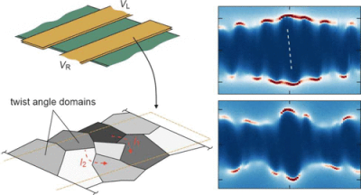
Nano Letters 26, 2119 (2026) We report low-temperature measurements of two adjacent, gate-defined Josephson junctions (JJs) in magic-angle twisted bilayer graphene (MATBG) at a moiré filling factor near ν = -2. We show that both junctions exhibit a prominent, gate-tunable Josephson diode effect, which we explain by a combination of large kinetic inductance and non-uniform supercurrent distribution. Despite their proximity, the JJs display differences in their interference patterns and different diode behavior, underscoring that microscopic inhomogeneities such as twist angle variations shape the non-uniform supercurrent and drive the diode behavior. As a result, the nonreciprocal supercurrent can be tuned by gate voltage, enabling tuning of the diode efficiency and even reversing the polarity at fixed magnetic fields. Our findings offer potential routes for tailoring Josephson diode performance in superconducting quantum circuits.
05.02.2026
Special Teaching Award for phyphox
Our phyphox team has received the RWTH Aachen Special Teaching Award in recognition of the impact and meaning of the physics teaching app phyphox.
You can find more details in the official RWTH article “How fast does the roller coaster accelerate? Your smartphone knows.”
23.01.2026
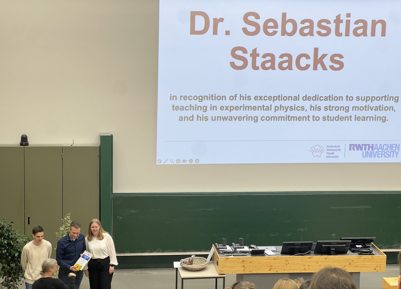
Sebastian Staacks Receives Physics Teaching Award 2026
Sebastian Staacks has been awarded the Physics Teaching Award for Supporting Teaching 2026 by the Fachschaft Physik RWTH Aachen. The award recognizes his exceptional dedication to teaching in experimental physics, his strong motivation, and his unwavering commitment to student learning at RWTH Aachen University. We congratulate Sebastian on this well-deserved award!
19.01.2026
The Profile Area MatSE supports the 38th IWEPNM in Kirchberg 2026
The Profile Area Materials Science and Engineering (MatSE) of RWTH Aachen University supports the 38th International Winterschool on Electronic Properties of Novel Materials (IWEPNM). The winter school will take place from February 28 to March 6, 2026, in Kirchberg/Tirol, Austria, bringing together leading researchers and young scientists to discuss recent advances in the electronic properties of novel materials.
Showing 1 - 8 (237 total) - Next