
Current events
Next talk on Friday in 4 days by Jonas Blum.
News 10.04.2026
New publication: Weak localization as a probe of spin-orbit-induced spin-split bands in bilayer graphene proximity coupled to WSe2
Site Content:
News 09.03.2021
New publication: How to solve problems in micro- and nanofabrication caused by the emission of electrons and charged metal atoms during e-beam evaporation
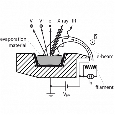
J. Phys. D: Appl. Phys. 54, 225304 (2021) We discuss how the emission of electrons and ions during electron-beam-induced physical vapor deposition can cause problems in micro- and nanofabrication processes. After giving a short overview of different types of radiation emitted from an electron-beam (e-beam) evaporator and how the amount of radiation depends on different deposition parameters and conditions, we highlight two phenomena in more detail: First, we discuss an unintentional shadow evaporation beneath the undercut of a resist layer caused by the one part of the metal vapor which got ionized by electron-impact ionization. These ions first lead to an unintentional build-up of charges on the sample, which in turn results in an electrostatic deflection of subsequently incoming ionized metal atoms toward the undercut of the resist. Second, we show how low-energy secondary electrons during the metallization process can cause cross-linking, blisters, and bubbles in the respective resist layer used for defining micro- and nanostructures in an e-beam lithography process. After the metal deposition, the cross-linked resist may lead to significant problems in the lift-off process and causes leftover residues on the device. We provide a troubleshooting guide on how to minimize these effects, which e.g. includes the correct alignment of the e-beam, the avoidance of contaminations in the crucible and, most importantly, the installation of deflector electrodes within the evaporation chamber.